
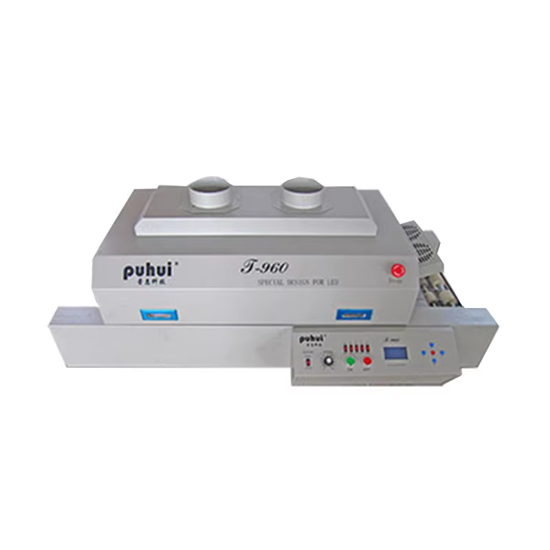
Revolutionize Your SMT Production: Advanced PCB Reflow Oven Solutions for Zero Defect Manufacturing
In today's ultra-competitive electronics field, PCB board warpage, component misalignment, and thermal inconsistencies in the soldering process can directly undermine yield and profitability. As board thicknesses are reduced to less than 0.4 millimeters and lead-free processes require extreme temperatures (240-250°C), traditional reflow soldering methods can fail catastrophically. The result? Production losses of up to 15% due to tombstoning, bridging and cold joints. With the global reflow oven market set to reach $2.1 billion by 2030 (at a CAGR of 7.5%), forward-thinking manufacturers can dominate their industries now with advanced thermal management technologies.
1. PCB Warping & Component Drop: The Silent Profit Killers
When an FR4 substrate exceeds its glass transition temperature (Tg) during reflow, it enters a rubber-like state and is susceptible to deformation. Thin boards (0.4-0.8 mm) collapse under gravity, misaligning solder joints. At the same time, heavy first side components fall off during the second reflow pass. Industry data shows:
63% of double-sided SMT failures stem from soldering defects caused by warpage
82% of connector breakout incidents occur during the second reflow process 134
2. Thermal inconsistency: a hidden defect generator
Uneven heating in low-cost ovens creates fatal temperature gradients:
Temperature differentials of ±15°C across the board → solder balling and voids
Slow heat-up → flux burning and delamination
Insufficient cooling → micro-cracks in BGA solder joints
16
May
23
Jun
23
Jun
23
Jun
Hunan Charmhigh provides top-notch SMT pick and place machines for electronics manufacturing. Our R&D-driven solutions and certifications ensure excellence. Contact us today!
No. 392, Minghu Road, Xiangjiang New Area, Changsha City, Hunan Province, China
Copyright © Hunan Charmhigh Electromechanical Equipment Co., Ltd. Privacy Policy
