
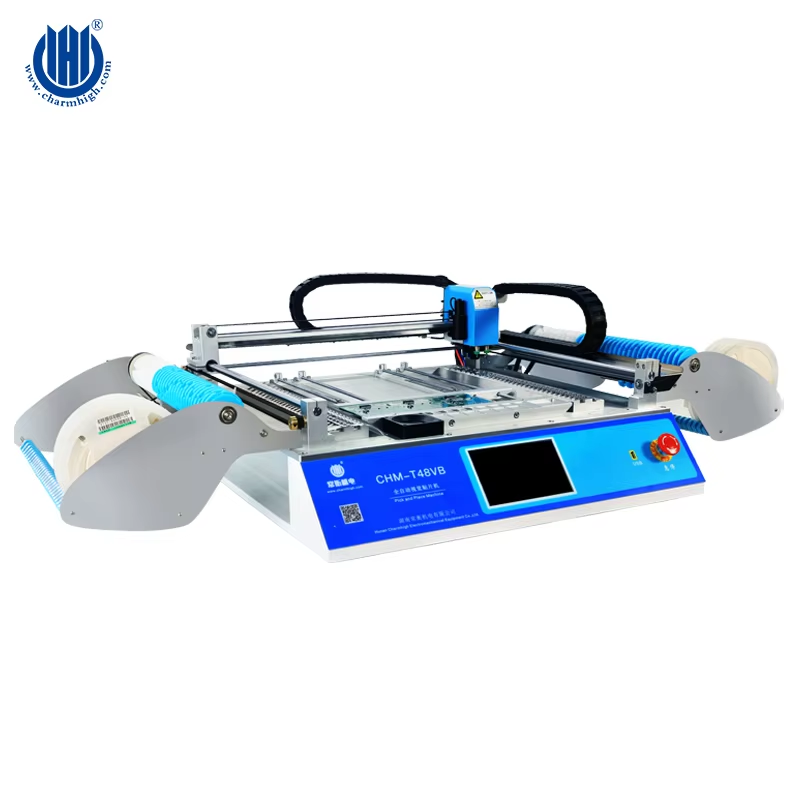
The Miniaturization Challenge in Modern About SMT Equipment
Trends Driving Component Miniaturization in Electronics Manufacturing
Consumer demand for lighter wearables, IoT sensors, and ultra-thin devices has reduced component sizes by 56% since 2019. Medical implants now require 0201-size SMD capacitors (0.2 × 0.1 mm), while automotive radar systems use 01005 inductors to save 34% PCB space compared to legacy designs. This shrink-to-innovate approach balances performance gains with spatial economy across industries.
Impact of 01005 Components and Micro-Scale SMDs on PCB Density
Deploying 01005 packages (0.4 × 0.2 mm) increases PCB component density by 4.8× but exposes limitations in traditional SMT equipment. A 2023 Ponemon Institute study found misaligned micro-SMDs cause 78% of defects in high-density boards, highlighting precision gaps in nozzle-centric pick-and-place systems.
| Feature | Traditional SMT | Modern SMT Requirements |
|---|---|---|
| Placement Accuracy | ±50 µm | ±15 µm (sub-01005 scale) |
| Vision Resolution | 10 MP | 25 MP + 3D Height Mapping |
| Minimum Component Size | 0402 | 008004 (0.25 × 0.125 mm) |
How High-Density PCB Design Challenges Traditional SMT Equipment Limits
Multilayer boards with 18 µm traces and 0.2 mm pitch BGAs strain stencil printers and reflow ovens designed for 0603 components. Thermal profiling mismatches in mixed-component PCBs cause solder void rates exceeding 12% when using decade-old SMT equipment.
Why Advanced SMT Equipment Is Essential for Next-Gen Miniaturized Assembly
Modern SMT systems integrate 30 µm laser-cut stencils, hybrid fiducial alignment, and AI-driven thermal compensators to achieve 99.992% micro-SMD placement accuracy. These systems reduce tombstoning risks by 63% in 01005 capacitors through real-time pad-level flux monitoring—a capability absent in pre-2015 platforms.
Precision Engineering: Evolution of High-Accuracy SMT Placement Systems
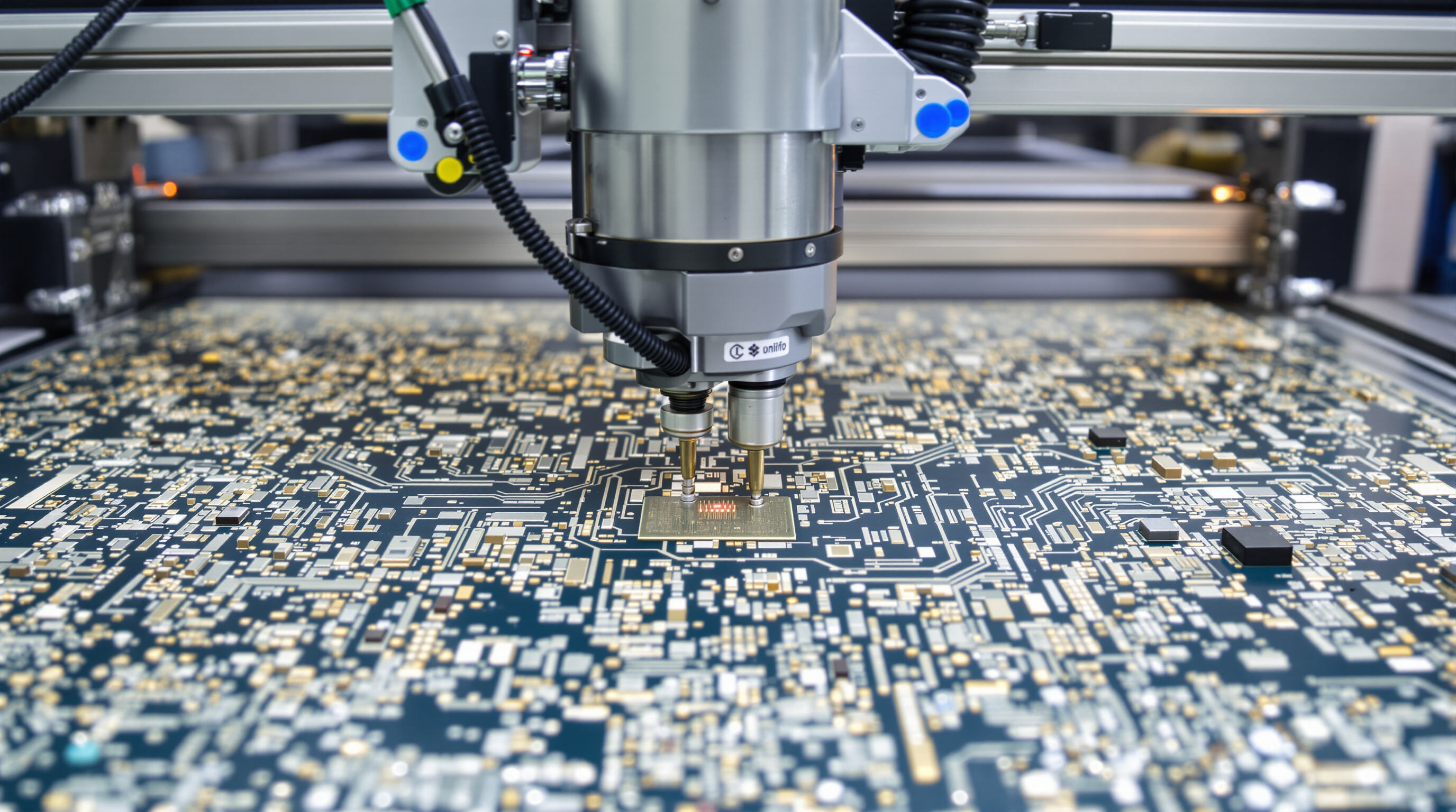
Advancements in Pick-and-Place Machine Capabilities and Precision
Today's surface mount technology (SMT) equipment reaches remarkable levels of precision thanks to advanced multi-head placement systems combined with smart motion controls. The latest generation of machines can hit around ±3 microns of accuracy dynamically, all while cranking out over 85 thousand parts each hour. That represents a massive jump forward compared to what was possible back in 2015. What makes these systems so effective is their integration of laser alignment for fiducial markers, which helps correct any warping issues in printed circuit boards. This feature becomes especially important when working with those super thin materials that measure less than 0.4 millimeters thick, something many manufacturers deal with regularly nowadays.
Sub-Micron Placement Accuracy and Its Role in Surface-Mount Device (SMD) Reliability
Sub-5µm placement accuracy reduces microvoids in solder joints by 63% compared to traditional systems, as demonstrated in thermal cycling tests under IPC-9701A standards. This precision prevents latent failures in 01005 capacitors used in 5G mmWave circuits, where 15µm misalignment can degrade signal integrity by 22dB at 28GHz frequencies.
Mechanical Innovations Reducing Vibration and Thermal Drift
Advanced SMT equipment employs carbon-fiber gantries with active vibration cancellation, reducing placement deviations to <0.8µm during 4m/s² accelerations. Dual-stage thermal compensation systems maintain ±1µm stability across 15–40°C operating ranges, addressing warpage in flexible hybrid electronics (FHE) assemblies.
Case Study: Achieving 99.99% Yield in Sub-0201 Component Placement
A Tier-1 automotive supplier implemented vision-guided robotic end effectors with 20MP coaxial illumination, achieving 0.7µm repeatability in 0.25mm pitch BGA placements. Their zero-defect production for ADAS modules required real-time solder paste inspection (SPI) feedback loops to placement heads, eliminating tombstoning in 0201 resistors.
Balancing Speed and Precision in High-Volume Miniaturized SMT Assembly
Next-gen SMT equipment resolves the speed-accuracy paradox through machine learning-optimized pick sequences. By analyzing 12,000 placement paths per hour, systems reduce non-value movements by 38% while maintaining <2µm positional drift. A 2024 IPC report shows these advancements enable 92% cycle-time reductions in smartwatch PCB production without compromising 99.95% first-pass yield thresholds.
Intelligent Vision and Inspection for Micro-Scale Accuracy
Role of High-Resolution Vision Systems in Detecting Micro-Scale Misalignments
Modern SMT equipment employs vision systems with 12MP+ cameras and 5µm/pixel resolution to detect misalignments smaller than 15µm—critical for 01005 components (0.4mm x 0.2mm). These systems achieve 99.95% detection accuracy through multi-spectral imaging that isolates solder paste variations from PCB substrate textures.
Multi-Angle Imaging and AI-Powered Defect Recognition in Complex PCBs
Leading systems now combine 360° oblique viewing with convolutional neural networks (CNNs) to identify tombstoning and solder bridges in dense BGA layouts. According to a 2025 Machine Vision in Electronics Report, AI-powered inspection reduces false positives by 62% compared to traditional algorithms when handling components below 0201 metric sizes.
Real-Time Feedback Loops Between Inspection and Placement Modules
Advanced SMT lines now synchronize inspection data with placement heads at 250ms intervals, enabling on-the-fly corrections for Z-axis pressure and nozzle rotation. This closed-loop system cuts placement errors by 41% in high-mix production environments.
How Smart Verification Enhances Overall SMT Equipment Performance
By integrating 3D solder paste inspection (SPI) with predictive analytics, modern systems achieve first-pass yields exceeding 99.2% for 0.35mm-pitch QFN packages. Real-time thermal compensation algorithms maintain ±3µm positional stability despite temperature fluctuations on the production floor.
AI-Driven Automation: Smarter Control in SMT Processes
Integration of AI in Optimizing Feeder Setup and Placement Trajectories
Modern SMT equipment leverages artificial intelligence to automate feeder replenishment schedules and optimize nozzle path planning. By analyzing historical production data, these systems reduce setup time by 22% while minimizing collisions in high-density PCB layouts, as shown in recent process control studies.
Machine Learning Models Predicting Component Warpage and Tombstoning Risks
Deep learning algorithms process thermal imaging and material property data to forecast solder joint failures before placement occurs. A 2023 industry analysis found manufacturers using predictive analytics achieve 41% fewer tombstoning defects in 01005 components compared to conventional methods.
Adaptive Calibration Systems Responding to Environmental Fluctuations
Self-adjusting vision systems compensate for factory floor vibrations (±0.5µm accuracy) and temperature swings (0.02°C resolution) through continuous IoT sensor feedback. This real-time adaptation maintains placement precision below 15µm CpK even in non-climate-controlled environments.
Addressing the Controversy: Over-Reliance on Automation in Critical Micro-Assembly Stages
While AI-driven SMT equipment delivers unmatched consistency in mass production, experts caution against full automation for prototype assemblies. A balanced approach preserves human oversight for validating first-article components while deploying machine learning for volume runs exceeding 10,000 units.
Material, Process, and Future Frontiers in SMT Technology
Solder Paste Deposition Challenges for Ultra-Fine Pitch Components
Today's surface mount technology (SMT) equipment must handle solder paste application for components with incredibly small pitches, sometimes less than 0.3mm apart. As manufacturers move toward using those tiny 01005 package sizes, they need to deposit solder paste in amounts under 0.4 cubic millimeters. Getting this right is tricky because alignment has to be spot on within about 12.5 micrometers either way, otherwise we end up with solder bridges or weak connections. According to recent research from the IPC in 2023, roughly one third of all problems in micro soldering come down to inconsistent paste behavior. This has led to some interesting developments in the field, particularly pressure controlled jet dispensing systems which can maintain consistent results over 99 times out of 100, even when working with stencils as narrow as 75 micrometers across.
Stencil Technology Advancements Enabling Consistent Micro-Aperture Filling
Laser-cut electroformed nickel stencils now achieve 1:3 aspect ratios for apertures down to 30µm, compared to conventional 1:5 limitations. Nano-coating treatments reduce paste adhesion by 62% (SMTnet 2024), while machine vision-driven auto-cleaning systems maintain aperture integrity during high-volume production runs. These advancements support 5G infrastructure manufacturing, where component densities exceed 250/cm².
Thermal Profiling Complexities in Reflow Ovens for Heterogeneous Component Arrays
Optimizing reflow parameters for mixed-mass assemblies requires balancing:
| Challenge | Solution | Result |
|---|---|---|
| ±1.5°C temp differentials | 12-zone convection systems | 94% reduction in voiding |
| Warpage in 0.1mm substrates | Adaptive nitrogen purge control | 0.003mm max deflection |
Advanced thermal mapping algorithms now compensate for board-level thermal mass variations in real time.
Next-Generation SMT Equipment With Dynamic Realignment and Predictive Maintenance
AI-driven placement heads now perform 1200±0.8µm corrections/second during component descent, addressing warpage detected by in-situ 3D scanners. Predictive maintenance systems analyze 14 equipment parameters to forecast nozzle wear 48 hours in advance, reducing unplanned downtime by 83% (2024 NPI Report).
Convergence of Additive Manufacturing and SMT for Embedded Components
Hybrid production lines now embed 0201 resistors within 3D-printed dielectric layers before final SMT assembly. This approach reduces interconnect lengths by 60% while enabling 22% smaller form factors in RF modules, as validated by recent 5G front-end module prototypes.
FAQ
What are 01005 components?
01005 components are extremely small surface-mount devices typically measuring 0.4 x 0.2 mm, widely used in high-density electronics manufacturing for saving PCB space.
Why is precision important in SMT placement systems?
Precision reduces defects such as microvoids in solder joints and prevents signal degradation, crucial for applications like 5G mmWave circuits.
How does AI improve SMT processes?
AI optimizes feeder setups, predicts tombstoning risks, and maintains precision amidst environmental fluctuations, thereby reducing defects and downtime.
What advancements support micro-aperture filling?
Laser-cut electroformed stencils and nano-coating treatments have improved the accuracy and consistency of solder paste deposition in ultra-fine components.
Table of Contents
- The Miniaturization Challenge in Modern About SMT Equipment
-
Precision Engineering: Evolution of High-Accuracy SMT Placement Systems
- Advancements in Pick-and-Place Machine Capabilities and Precision
- Sub-Micron Placement Accuracy and Its Role in Surface-Mount Device (SMD) Reliability
- Mechanical Innovations Reducing Vibration and Thermal Drift
- Case Study: Achieving 99.99% Yield in Sub-0201 Component Placement
- Balancing Speed and Precision in High-Volume Miniaturized SMT Assembly
- Intelligent Vision and Inspection for Micro-Scale Accuracy
-
AI-Driven Automation: Smarter Control in SMT Processes
- Integration of AI in Optimizing Feeder Setup and Placement Trajectories
- Machine Learning Models Predicting Component Warpage and Tombstoning Risks
- Adaptive Calibration Systems Responding to Environmental Fluctuations
- Addressing the Controversy: Over-Reliance on Automation in Critical Micro-Assembly Stages
-
Material, Process, and Future Frontiers in SMT Technology
- Solder Paste Deposition Challenges for Ultra-Fine Pitch Components
- Stencil Technology Advancements Enabling Consistent Micro-Aperture Filling
- Thermal Profiling Complexities in Reflow Ovens for Heterogeneous Component Arrays
- Next-Generation SMT Equipment With Dynamic Realignment and Predictive Maintenance
- Convergence of Additive Manufacturing and SMT for Embedded Components
- FAQ