
Электроника өндіру машиналарының негізгі сатыларын түсіну: Электроника өндіру машиналары
Жобадан жеткізуге дейін: Толық өндіріс ағынын картаға түсіру
Қазіргі заманның электрондық құрылғыларын жасау процесі, әдетте, алдымен 3D модельдер жасау мен тәжірибелік үлгілер дайындаудан басталады. Инженерлер осындай абстрактты идеяларды шынығы жұмыс істейтін нәрсеге айналдырады. 2024 жылғы аяқ киім өндіруде қолданылатын материалдар туралы соңғы есепке сәйкес, осындай күрделі дизайн бағдарламаларын қолданатын компаниялар өздеріне ұқсас салалардағы басқа компаниялармен салыстырғанда шамамен 18% аз материал қалдырады. Бұл бастапқы кезеңде бәрін дұрыс жасаудың қаншалықты маңызды екенін көрсетеді. Тестілеу кезінде бәрі қанағаттанарлық болғаннан кейін, өндірушілер автоматтандырылған жүйелерді қолданып, печаттық платаларды, компоненттерді орнату мен бөлшектерді дәнекерлеу үшін өндірісті кеңейтеді. Содан кейін тауарлар тұтынушыларға жеткенде бәрі сенімді жұмыс істеуі үшін әртүрлі тексерулер мен сынақтар жүргізіледі.
Печаттық платаларды өндіру мен жинау кезеңдері
ППТ жасау ламинацияланған материалды дайындаудан басталады, одан кейін мыс әбдендеу процесіне, тесіктерді тесуге және қорғауыш қабаттарды салуға көшіледі. Беттік орнату құрылғыларын орнату кезінде өндірушілер жиі микрон деңгейінде өте жоғары дәлдікті қамтамасыз ететін компьютерлік көру технологиясымен басқарылатын роботтық жүйелерге сүйенеді. Жасау үшін ыңғайлылықты тексеру өндіріс басталмай-ақ потенциалды жинау проблемаларының жартысынан екі үшіне дейінгісін анықтайды, бұл көптеген салалық сарапшылардың байқауларына негізделген. Сызықтың соңында плата қорғауыш материалдармен жабылады және сигналдар дұрыс жұмыс істейтінін және әртүрлі орташа жағдайларға шыдайтынын қамтамасыз ету үшін қатаң тестілеуден өтеді.
Қазіргі заманғы желілердегі электроника өндіру машиналарының рөлі
Орташа көлемдегі өндіруде автоматтандырылған pick-and-place жүйелері SMD компоненттерінің 98%-ын өңдейді және сағатына 25 000-нан астам орнатулар жылдамдықпен жұмыс істейді. Тұйық циклді жылулық профильдеуі бар рефлоу пештері ±1,5°C дәлдікпен температураны ұстайды — бұл қорғасыз дәнекерлеу қосылыстарының сенімділігі үшін маңызды. Бұл жаңартулар жартылай автоматтандырылған желілерге қарағанда қолмен кірісуге 75% аз қажеттілік туғызады және тұрақтылық пен өткізу қабілетін айтарлықтай арттырады.
Зерттеу жағдайы: Орташа масштабтағы электроника зауытындағы жұмыс үдерісін оптимизациялау
Орталық Америкадағы бір өндіруші solder paste printing және reflow сатыларынан кейін бағдарланған AOI жүйелерін енгізу арқылы циклдық уақытты 40% жақсартты. Нақты уақыт режиміндегі ақауларды анықтау қайта өңдеу шығындарын жылына $140 мыңға төмендетті, бұл кезеңдік автоматтандыру жаңартуларының инвестициядан түсетін пайданы көрсетеді.
Бағыт: Масштабталатын шығарылым үшін Smart Manufacturing технологияларын интеграциялау
Жетекші қондырғылар қазір IoT-мен жабдықталған жабдықтарды болжау аналитикасымен үйлестіре отырып, жабдықтардың 92% дейінгі уақытта жұмыс істеуін қамтамасыз етеді. Осы ақыллы өндіріс тәсілі тұтынушылық электроника сұранысының өзгеріп отыруын қанағаттандыру үшін маңызды мүмкіндік болып табылатын өнімдерді тез ауыстыруды мүмкін етеді.
Өндіруге Арналған Дизайн (DFM) және Өндірістен Бұрынғы Жоспарлау
Қателерді болдырмау үшін Gerber Файлдары мен DFM Талдауын Пайдалану
Бастапқы кезде дұрыс дизайн файлдарын алу өндірістегі қателерді болдырмау үшін компанияларға кейіннен үлкен сома ақша үнемдетуі мүмкін. Көбінесе PCB мамандары дизайнерлер мен зауыттың өндіріс жоспары арасындағы ортақ тіл ретінде RS-274X пішіміндегі Gerber файлдарына сүйенеді. Бұл файлдар негізінен мыс элементтердің орнын, тесіктердің қалай дәлеленуі керектігін және қорғаныш қабаттарының қай жерге орналасуы керектігін көрсетеді. Қазіргі заманғы «ақылды» зауыттар компьютерлік тексеруді шын мәніндегі инженерлермен біріктіріп, тесіктердің айналасындағы сақиналардың тым кішкентай болуы немесе трассалардың бір-біріне тым жақын өтуі сияқты ерте сатыдағы мәселелерді анықтайды. Өткен жылы жүргізілген кейбір зерттеулер қатты әсер қалдырды — компаниялар дизайнды тексеру үшін AI құралдарын қолданса, тек қана адамдар тексергенге қарағанда тақталарды қайта жасау қажеттілігі 62% кем болды.
Жиі кездесетін PCB дизайнының қателіктері және DFM оларды қалай болдырмауға көмектеседі
Өндіріске дейінгі кезеңде үш негізгі қиындық басымдық танытады:
- Импеданс сәйкессіздіктері бақыланбайтын трасса геометриясынан туындайды
- Жылулық кернеу салдарынан болатын істен шығулар дұрыс емес виа орналасуына байланысты
- Жинау кемшіліктері дәл жеткіліксіз қорғау қабатының таралуынан туындайды
DFM протоколдары өндірістік дәлдікті қамтамасыз ету үшін автоматтандырылған дизайн ережелерін тексеру (DRC) арқылы осы мәселелерді шешеді. Мысалы, беткі орнату пішіндері рефлоу печьтерінің жылулық модельдеу деректеріне негізделе отырып түзетіледі, бұл құйма қалайының көлемі мен буын сенімділігін оптимизациялауға мүмкіндік береді.
Сапаны қамтамасыз ету үшін инновацияны стандарттаумен тепе-теңдікте ұстау
Жоғары тығыздықты қосылыстар мен жаңаша пакеттер заманауи дизайндарды мүмкіндік етсе де, DFM негізгі элементтерді стандарттаудың маңызын атап көрсетеді. IPC-7351B контактілік үлгі кітапханалары мен JEDEC компонент контурлары электроника өндірісінің әртүрлі жабдықтарымен сәйкестікті қамтамасыз етеді. Бұл негіз пайдаланылуын азайтпай, пассивті элементтердің орнатылуы немесе гибридті SMT-THT конфигурациялары сияқты мүмкіндіктерді қолдауға мүмкіндік береді.
Материалдар тізбесі (BOM) және стратегиялық компоненттерді табылуы
Дизайн мен өндіріс қажеттіліктерін сәйкестендіру үшін дәл материалдар тізбесін жасау
Материалдардың дәл шоты немесе BOM нақты зауытта қалай жасалатынын қағазда қалай жобаланғанымен шынымен байланыстырады. BOM-да резисторлар, конденсаторлар, тіпті барлығын бекітетін кішкентай бұрандалар сияқты үлкенірек және кіші компоненттердің барлығы тізілген болуы керек. Біз кішкентай детальдарды қосып, сонымен қатар нұсқаларды дұрыс есепке алу арқылы жинау қателерін шамамен 30-35% азайтқан цехтарды көрдік. Жақсы мысалдар үшін Fictiv-тің қолайлы материалдар нұсқаулығын қараңыз. Олар әртүрлі кезеңдерде стандартты бөлшек нөмірлерін қолданудың прототиптер тамаша көрінетін, бірақ бірнеше мың бірлікті шығару кезінде сәйкес келмейтін жағдайларды қалай болдырмауға болатынын көрсетеді. Мұндай тұрақтылық кейін орын алатын қиындықтарды болдырмақ үшін қажет.
Жеткізушіні таңдау: Құнын, әзірлеу уақытын және MOQ-ды бағалау
Өндірісте компоненттерді таңдаған кезде компаниялардың әрбір бөлшектің құнын, бірден қанша тапсырыс беру қажеттігін және жеткізу уақытын салыстырып отыруы керек. Мысалы, конденсаторларды алып отырсақ – бір бөлшек 20 пайызға арзан болса, бірақ оның жеткізілуіне 12 апта кететінін білгенде, бұл өндірістің уақыт кестесін үлкен қиындыққа түсіруі мүмкін. Көбінесе сатып алу бөлімдері ақаулық деңгейі (әдетте 0,5 пайыздан төмен болуы керек) мен тауарлардың уақытылы жеткізілуі сияқты көрсеткіштерді бақылау үшін жеткізушілерге арналған бағалау карталарын пайдаланады. Толық маңызды негізгі бөлшектер үшін көптеген өндірушілер екі жеткізушіден тәуелді болу стратегиясын қабылдайды. Бұл тәсіл операцияларды кеңейткен кезде қауіп-қатерді шашыратуға көмектеседі және тізбекті жеткізу саласындағы мамандардың көбісі бүгінгі таңда өндіріс орталықтарында бұл практиканың стандартты деп санайтынын мойындайды.
Шаруашылық ішіндегі сатып алу мен EMS-ке жеткізу: Артықшылықтары, кемшіліктері және алмастырулар
Компаниялар сатып алу операцияларын өз қолдарында ұстаған кезде, өнім сапасын бақылау мүмкіндігі жақсаяды, бірақ осының құны көбінесе елемеуге болмайтындай болып келеді. Орташа масштабтағы бизнеске тиісті мөлшерде өнім қорын ұстау үшін жарты миллион доллар немесе одан да көбін бөлу қажет болады. Екінші жағынан, Электроникалық Өндіріс Қызметтерімен (EMS) жұмыс істеу материалдарға деген шығындарды 15%-дан 30%-ға дейін қысқартуға мүмкіндік береді. Алайда, бәрі қалай өзгерістер енгізуді ұнатса да, үшінші тарап арқылы жүргізілетін өзгерістер уақытты көбірек алады. Әр ай сайын шамамен 50 мың бірлік өнім шығаратын ірі өндірушілер ортақ шешімге келді. Брендінің ерекшелігін анықтайтын ерекше бөлшектерді компания шеңберінде өздері жинақтап, ал қалған стандартты бөлшектерді контракттық өндірушілерге жібереді. Дәл осылайша, өндіріс әлемінде бәрін қолыңнан келтіруге болады.
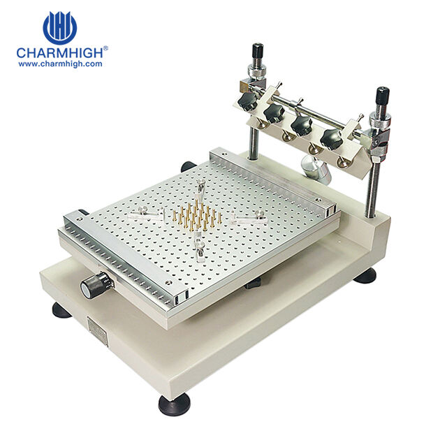
PCB Жинақтау Әдістері және Электронды Өндіріс Машиналары арқылы Автоматтандыру
Беткі орнату технологиясы (SMT): Жоғары жылдамдықты дәлме-дәл жинау
Қазіргі уақытта басылып шығарылған электрондық плата (ПЕП) жинау үшін Беткі орнату технологиясы (SMT) негізгі әдіс болып табылады. Бұл 0,4 на 0,2 миллиметр өлшемді 01005 резисторлар сияқты өте кішкентай компоненттерді сағатына 25 мыңнан астам орналастыру жылдамдығымен орналастыруға мүмкіндік береді. Соңғы үлгідегі көруі бар роботтар бөлшектерді шамамен 30 микрометрге дейінгі дәлдікпен орналастыра алады және ескі әдістермен салыстырғанда адамның жасауы мүмкін қателіктерді шамамен 92 пайызға қысқартады. Бұл осындай жоғары дәлдіктің арқасында аккурат сағаттар мен интернетке қосылатын басқа да құрылғылар сияқты кішігірім электроникалық құрылғыларды құрастыруды мүмкін етеді және тақталарды өндіру циклын көбінесе он бес секундтан кем болатындай етіп ұстауға мүмкіндік береді.
Тесік арқылы орнату технологиясы (THT) және қолмен дәнекерлеу қолданбалары
Сенімділік мәні зор қолданыстарда, мысалы, автомобиль басқару жүйелері мен ауыр өнеркәсіптік электр жабдықтарында сквозной орнату технологиясы әлі де белгілі бір орын алады. Шағын сериялы PCB өндірісте тақталардың әрбір бестен бірі қолмен дәнекерленеді, әсіресе 2 ватттан астам қуатты бөлшектер немесе қосымша механикалық беріктік қажет болған кезде. Көптеген өндірушілер шын мәнінде қазіргі уақытта гибридті жинау жолақтарын жүргізеді, сквозной және беттік орнату әдістерін араластыра отырып, екеуінің де артықшылықтарын пайдаланады. Әскери стандарттағы схемалық тақталар осы тәсілдің қалай жақсы жұмыс істейтінінің негізгі мысалы болып табылады. Оларда күшті тербелістерге (50G-ге дейін) төзімді сквозной коннекторлар жиі қолданылады, ал дәлме-дәл сигналдарды өңдеу міндеттері үшін беттік орнатылатын чиптерге сүйенеді.
Рефлоу мен толқынды дәнекерлеу: Дұрыс әдісті таңдау
| Әдісі | Ең жақсы | Термиялық тұрақтылық | Өткізу қабілеті (тақталар/сағат) |
|---|---|---|---|
| Рефлоуздық жалғау | 0201+ компоненттері бар SMT тақталары | аймақтар бойынша ±2°C | 120–160 |
| Толқынды дәнекерлеу | Аралас технологиялық тақталар | дәнекерлеу ваннасында ±5°C | 80–100 |
Азотты атмосферасы бар рефлоу-пештері ұсақ қадамды жалғауларда (<0,3 мм) тотығуды минималдандырады, ал толқындық жүйелер термиялық циклдауға төзімділікті талап ететін аралас технологиялық тақталар үшін өте жақсы көрсеткіш береді.
Зерттеу жағдайы: Автоматтандырылған SMT желісін енгізу
Орташа көлемді электроника өндірушілердің бірі жаспаушы трафаретті принтерлер, SPI жүйелері және 8 аймақты рефлоу-пештері бар жаңа 5 сатылы беттік орнату технологиясы желісін орнатқаннан кейін жинау құнын жуық 40% дейін төмендетті. Бірінші өту нәтижесі пайдалы өнім 82%-дан 96%-ға дейін секірді, негізінен нақты уақыт режиміндегі қорғасын қоспасын тексеру мен ақауларды автоматтандырылған оптикалық тексеру арқасында. Бұл ғана айына қателерді түзетуге кететін уақытты шамамен 64 сағатқа үнемдеуге мүмкіндік берді. Олар қосымша зауыт кеңістігін қажет етпей-ақ күн сайын 8 500 электрондық схема тақтасын шығара алатын болғаны да таңғаларлық. Қазіргі кезде көптеген компаниялар осындай жоғары технологиялық өндірістік жабдықтарға инвестиция салуы түсінікті.
Тестілеу, сапа қамтамасыз ету және үздіксіз өндірістің оптимизациялануы
AOI, ICT және нақты уақытта сапаны бақылау жүйелерін енгізу
Өндірушілер автоматтандырылған оптикалық тексеруді (AOI) тізбектегі тестілеумен (ICT) бірге қолданған кезде, әдетте ақаулар деңгейі 0,5%-ден төмен түседі. Бұл технологияларды шығару кезінде пайда болатын сапа мәселелерінің шамамен 34% азайғанын хабарлайды. Тексеру жүйелері бұйымдардың орналасуы мен тізбектің жұмысынан бастап дәнекерлеу қосылыстарына дейін бәрін тексереді және сағатына 25 мыңнан астам тест жүргізе алады. Көптеген алдыңғы қатарлы өндірушілер үлкен сериялы өндіріс кезінде өндірістік параметрлерді плюс-минус 1,5% ішінде тұрақты ұстау үшін статистикалық процесті басқару панелдеріне сүйенеді. Мыңдаған бұйымдарды күн сайын жинау жолдарымен өткізген кезде осындай дәлдік маңызды рөл атқарады.
Автоматтандырылған оптикалық тексеру (AOI) арқылы ақауларды азайту
2023 жылғы PCB өндіру бенчмаркетіне сәйкес, рефлоулық пісіруден кейін орнатылған AOI жүйелері мостиктер немесе тасбақа тәрізді болып кету сияқты өте маңызды ақаулардың 98,7%-ын анықтайды. Тығыз орналасқан немесе миниатюризацияланған блоктарда әсіресе, тарихи ақау үлгілерін талдау арқылы машиналық үйрену алгоритмдері жыл сайын анықтау дәлдігін 12% жақсартады.
Мәліметтерге Негізделген Тиімділік: Шығым Көрсеткіштерін Бақылау және Тоқтап Қалуларды Азайту
IoT-мүмкіндік беретін талдау платформалары жылулық профильдер мен конвейер жылдамдықтарын қоса алғанда, 18-ден астам өнімділік көрсеткіштерін бақылайды. Болжау сипатындағы техникалық қызмет көрсетуді қолданатын өндірушілер Понеман институтының 2023 жылғы деректері бойынша, күтпеген тоқтап қалулар 41% аз болып табылады және күрделі блоктарда бірінші өтудегі шығым 94% асып түседі.
Күрделі Электроника Өндіру Жабдықтарымен Өндірісті Масштабтау
Автоматтық калибрлеуі бар модульді SMT желілері өнімді тез ауыстыруды қамтамасыз етеді және дайындау кезіндегі шығынды 28% азайтады. Екі желілі принтерлер мен гибридті орналастыру құрылғылары сағатына 38 000 компонентті 15¼м дәлдікпен өңдейді — бұл сенімділік пен қайталану мүмкіндігі маңызды болып табылатын автомобильжәне медициналық құрылғылар өндірісі үшін маңызды.
Жиі қойылатын сұрақтар (ЖҚС)
Электроника өндірісінің негізгі кезеңдері қандай?
Негізгі кезеңдерге дизайн мен прототиптеу, PCB өндірісі, жинау, тексеру және сапа мен сенімділікті қамтамасыз ету үшін соңғы жеткізу кіреді.
Өндіруге арналған дизайн (DFM) процесі қалай жұмыс істейді?
DFM потенциалды қателерді тексеру үшін Gerber файлдары сияқты дизайн файлдарын қолдануды қамтиды. Автоматтандырылған дизайн ережелерін тексеру жиі кездесетін қателерді анықтайды және жинау кезіндегі мәселелерді болдырмау үшін дизайндарды түзетеді.
Өндірісте материалдар кітапшасының (BOM) маңызы қандай?
Дәл BOM дизайнды өндіру қажеттіліктерімен сәйкестендіреді, барлық компоненттер мен түзетулерді тіркейді және тұрақтылықты қамтамасыз етеді, жинау қателерін азайтады.
Автоматтандырылған оптикалық тексеру (AOI) жүйелерін қолданудың пайдасы қандай?
AOI жүйелері рефлоу процесінен кейін тарихи үлгілерді машиналық үйрену арқылы талдау арқылы ақаулардың деңгейін едәуір төмендететін, жоғары дәлдікпен маңызды ақауларды анықтайды.
Мазмұны
-
Электроника өндіру машиналарының негізгі сатыларын түсіну: Электроника өндіру машиналары
- Жобадан жеткізуге дейін: Толық өндіріс ағынын картаға түсіру
- Печаттық платаларды өндіру мен жинау кезеңдері
- Қазіргі заманғы желілердегі электроника өндіру машиналарының рөлі
- Зерттеу жағдайы: Орташа масштабтағы электроника зауытындағы жұмыс үдерісін оптимизациялау
- Бағыт: Масштабталатын шығарылым үшін Smart Manufacturing технологияларын интеграциялау
- Өндіруге Арналған Дизайн (DFM) және Өндірістен Бұрынғы Жоспарлау
- Материалдар тізбесі (BOM) және стратегиялық компоненттерді табылуы
- PCB Жинақтау Әдістері және Электронды Өндіріс Машиналары арқылы Автоматтандыру
- Тестілеу, сапа қамтамасыз ету және үздіксіз өндірістің оптимизациялануы
- Жиі қойылатын сұрақтар (ЖҚС)